E-beam and ion beam applications
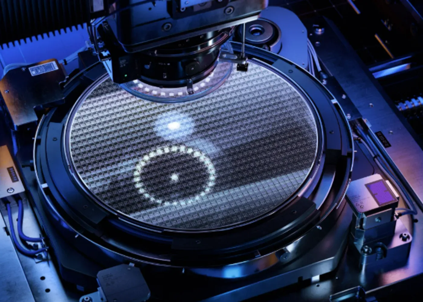
Electron beam (E-beam) technology is widely used in direct write lithography systems. One or multiple E-beam columns write ultra-fine patterns directly onto a reticle or wafer. This enables high-resolution patterning without the need for masks. E-beams are also applied in advanced microscopy and metrology, to inspect and measure reticles, wafers and other critical parts with nanometer accuracy.
Ion beam systems are used for material analysis and modification at atomic level. Applications include imaging, milling, deposition and circuit editing. These technologies are essential in both R&D and high-volume semiconductor manufacturing. Within these machines, environmental conditions are extremely demanding: ultra-high vacuum levels, temperature stability and vibration control are critical for process stability and repeatability.
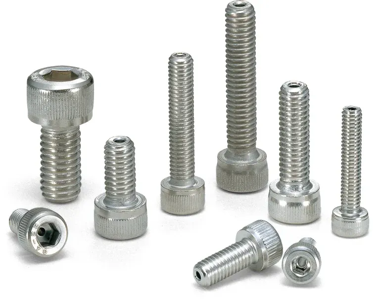
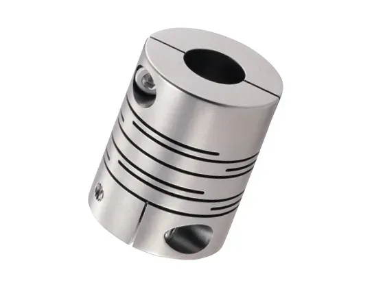
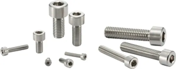
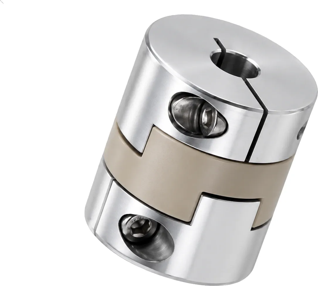
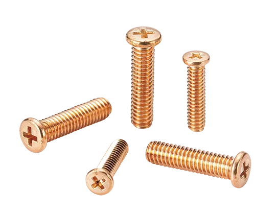
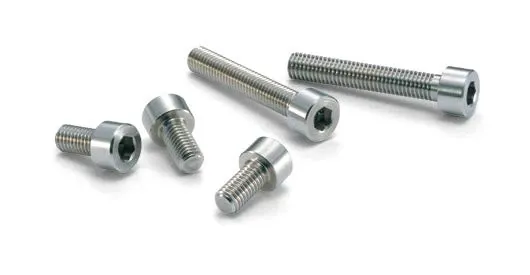
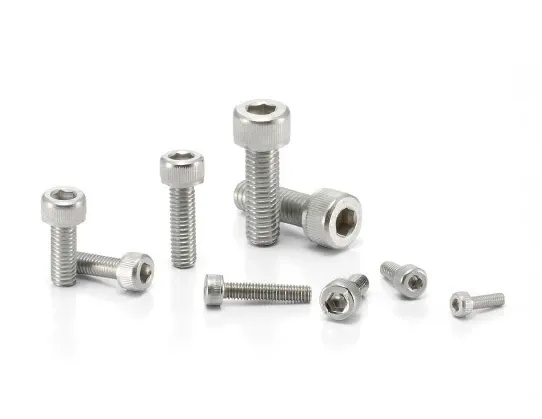
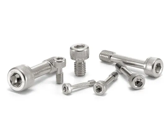
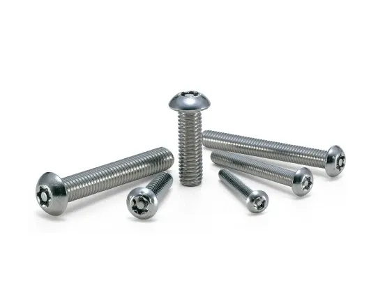
Material selection therefore plays a key role. Components must not interfere with the beam or the process. Non-magnetic materials are often required, as magnetic fields can deflect an E-beam and negatively affect positioning accuracy on the reticle or wafer. Low outgassing materials are essential to maintain vacuum quality and prevent contamination. NBK offers non-magnetic and corrosion-resistant fasteners, vacuum-compatible screws with ventilation holes, low-outgassing materials and surface treatments, zero-backlash couplings for precise torque transmission, and stainless steel and special material components for cleanroom use.